← 7-Pin Lawn Mower Ignition Wiring – DIY Fix Guide! Lawn mower 7 terminal ignition switch wiring diagram E46 Heated Seat Wiring Diagram: Stay Warm on the Road! Bmw e46 heated seat wiring diagram » wiring digital and schematic →
If you are searching about PCB Layout Guidelines For High Speed Applications - HardwareBee you've visit to the right page. We have 25 Images about PCB Layout Guidelines For High Speed Applications - HardwareBee like LVDS: High Speed LVDS PCB Design Guidelines | MADPCB, FPGA - DAC LVDS 1.25GBPS PCB SKEW IMAGE - YouTube and also PCB Layout Guidelines For A Successful Design | Reversepcb. Read more:
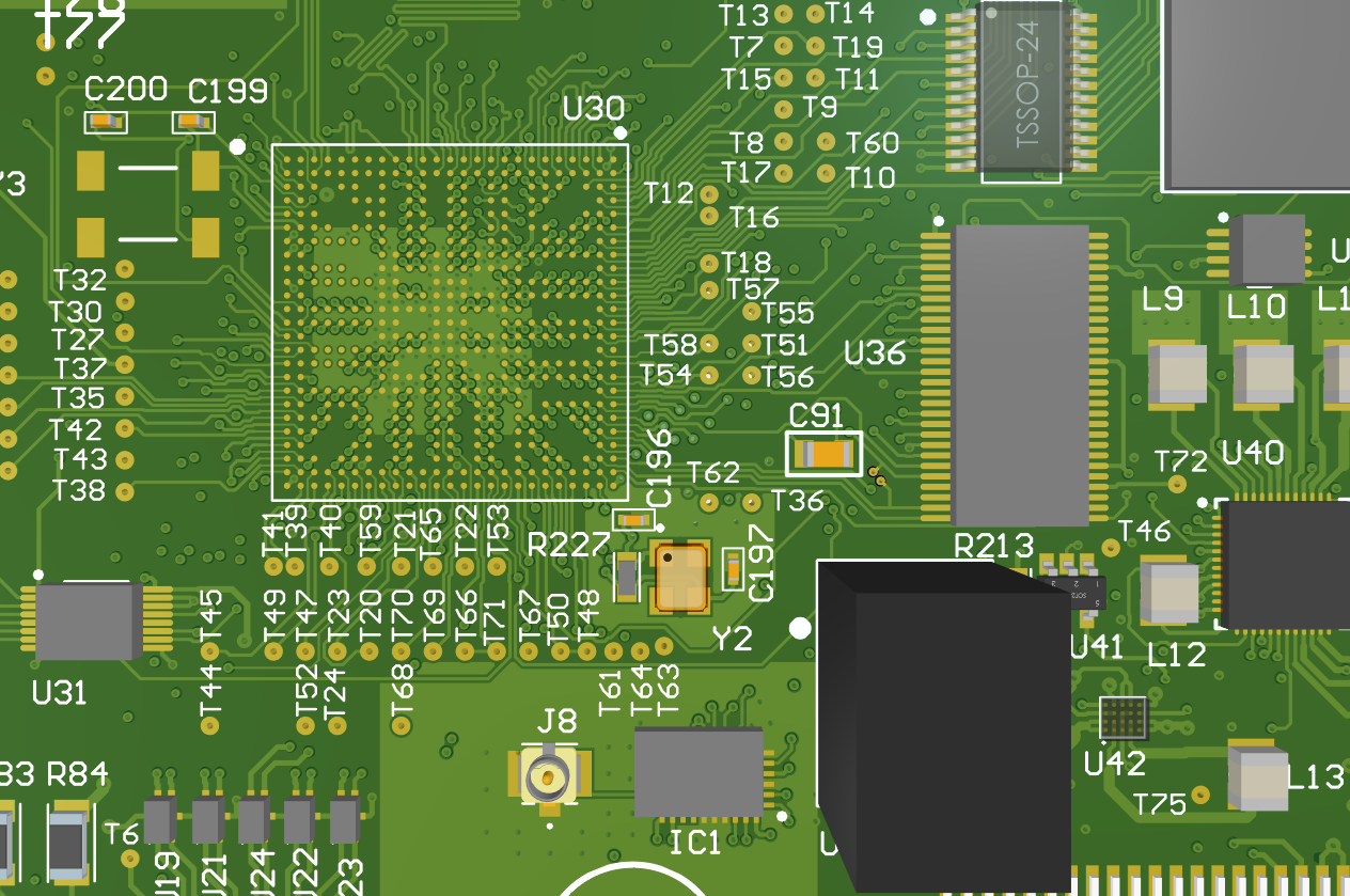
PCB Layout Guidelines For High Speed Applications - HardwareBee
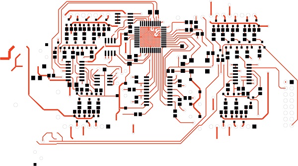 hardwarebee.com
PCB Layout Guidelines For High Speed Applications - HardwareBee
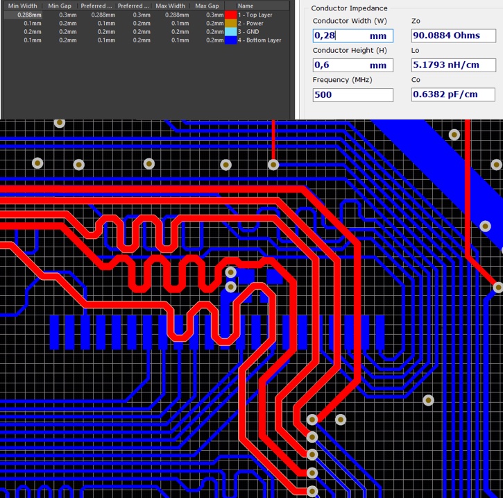
LVDS高速PCB布局布线设计_lvds等长差多少mil-CSDN博客
 blog.csdn.net
LVDS高速PCB布局布线设计_lvds等长差多少mil-CSDN博客
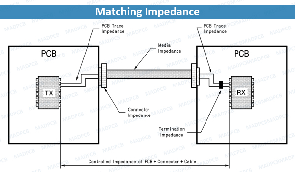
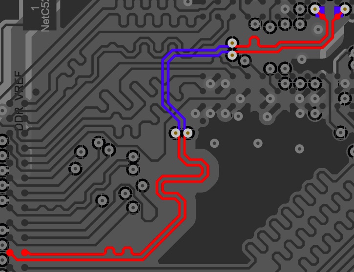
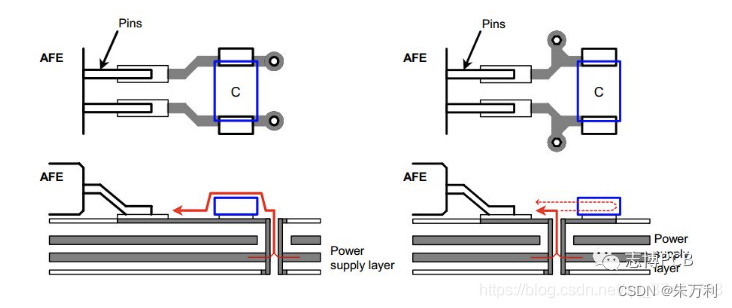
Some LVDS PCB Layout Guidelines For Ensuring Signal Integrity | PCB
Some LVDS PCB Layout Guidelines for Ensuring Signal Integrity | PCB ...
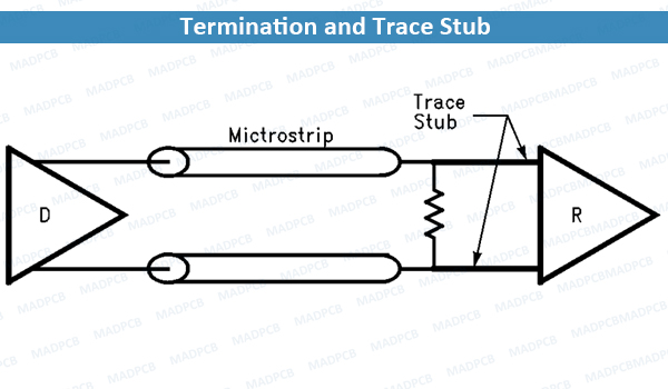
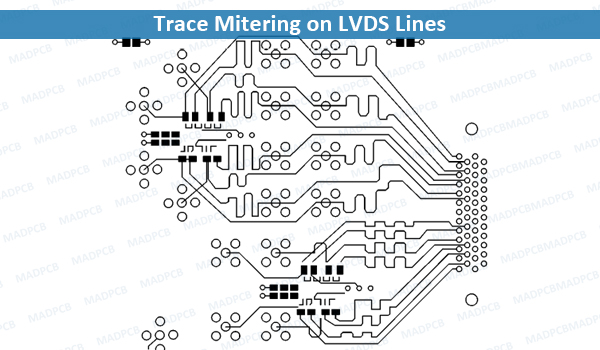
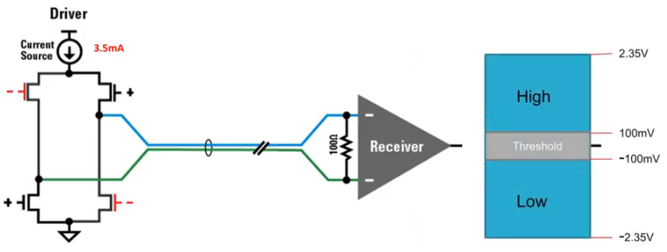
LVDS: High Speed LVDS PCB Design Guidelines | MADPCB
 madpcb.com
LVDS: High Speed LVDS PCB Design Guidelines | MADPCB
PCB Layout Guidelines For A Successful Design | Reversepcb
 reversepcb.com
PCB Layout Guidelines For A Successful Design | Reversepcb
FPGA - DAC LVDS 1.25GBPS PCB SKEW IMAGE - YouTube
 www.youtube.com
FPGA - DAC LVDS 1.25GBPS PCB SKEW IMAGE - YouTube
LVDS: High Speed LVDS PCB Design Guidelines | MADPCB
 madpcb.com
LVDS: High Speed LVDS PCB Design Guidelines | MADPCB
LVDS高速PCB布局布线设计_lvds等长差多少mil-CSDN博客
 blog.csdn.net
LVDS高速PCB布局布线设计_lvds等长差多少mil-CSDN博客
Main Design Guidelines & Layout Rules On High Speed PCB
 www.integrasources.com
Main Design Guidelines & Layout Rules on High Speed PCB
Main Design Guidelines & Layout Rules On High Speed PCB
 www.integrasources.com
Main Design Guidelines & Layout Rules on High Speed PCB
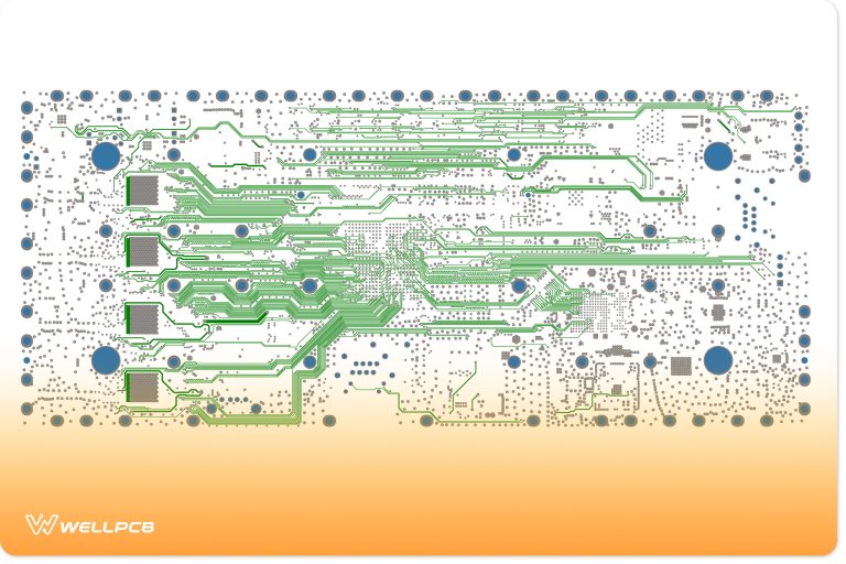
PCB Layout Guidelines | Design Rules & Requirements | Tips
 www.wellpcb.com
PCB Layout Guidelines | Design Rules & Requirements | Tips
PCB Design & PCB Layout : A Guide To Design The Right PCB
 www.hemeixinpcb.com
PCB Design & PCB Layout : A Guide To Design The Right PCB
Some LVDS PCB Layout Guidelines For Ensuring Signal Integrity | PCB
Some LVDS PCB Layout Guidelines for Ensuring Signal Integrity | PCB ...
PCB模块化设计12——LVDS高速PCB布局布线设计规范_22pin接口模块设计-CSDN博客
 blog.csdn.net
PCB模块化设计12——LVDS高速PCB布局布线设计规范_22pin接口模块设计-CSDN博客
PCB Layout Guidelines And Considerations
 www.microcontrollertips.com
PCB layout guidelines and considerations
A Detailed Guide To PCB Layout Design - IBE Electronics
 www.pcbaaa.com
A detailed guide to PCB layout design - IBE Electronics
Pcb Design & Layout, Your Expert For Pcb Design Service And Pcb Layout
 www.venture-mfg.com
Pcb Design & Layout, Your Expert For Pcb Design service and Pcb Layout ...
Some LVDS PCB Layout Guidelines For Ensuring Signal Integrity | PCB
 resources.altium.com
Some LVDS PCB Layout Guidelines for Ensuring Signal Integrity | PCB ...
LVDS: High Speed LVDS PCB Design Guidelines | MADPCB
 madpcb.com
LVDS: High Speed LVDS PCB Design Guidelines | MADPCB
PCB Layout Guidelines For A Successful Design | Reversepcb
 reversepcb.com
PCB Layout Guidelines For A Successful Design | Reversepcb
LVDS: High Speed LVDS PCB Design Guidelines | MADPCB
 madpcb.com
LVDS: High Speed LVDS PCB Design Guidelines | MADPCB
PCB Layout Guidelines | Design Rules & Requirements | Tips
 www.wellpcb.com
PCB Layout Guidelines | Design Rules & Requirements | Tips
Some LVDS PCB Layout Guidelines For Ensuring Signal Integrity | PCB
 resources.altium.com
Some LVDS PCB Layout Guidelines for Ensuring Signal Integrity | PCB ...
Top 5 PCB Design Rules You Need To Know | PCB Design Blog | Altium
 resources.altium.com
Top 5 PCB Design Rules You Need to Know | PCB Design Blog | Altium
18 PCB Layout Tips For Improving Your PCB Design And Reducing
 camptechii.com
18 PCB Layout Tips for Improving Your PCB Design and Reducing ...
Pcb layout guidelines for a successful design. Lvds: high speed lvds pcb design guidelines. Lvds高速pcb布局布线设计_lvds等长差多少mil-csdn博客